|
|
Your source of photonics CAD tools | |
|
| ||
PICWaveA photonic IC, laser diode and SOA simulator |
    |
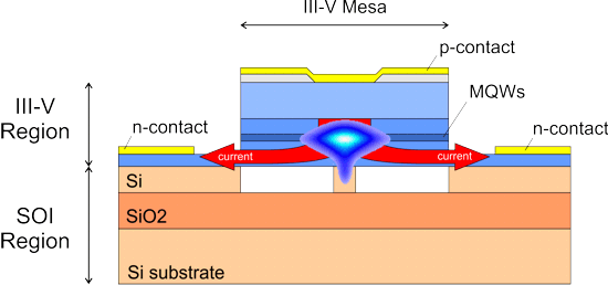
Hybrid Silicon Tapered Laser Diode (SOI)Simulation with PICWave softwarePICWave’s current spreading model allows the simulation of hybrid silicon laser diodes (or hybrid SOI laser diodes), where both n and p-contacts are on top, with lateral current flow from the central contact to those on the sides.
Hybrid silicon laser diodeThe figure below shows the setup of a hybrid silicon laser device in PICWave. The gain curves of the hybrid laser were generated using Harold and fitted in PICWave.
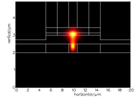
In this example, the silicon-on-insulator (SOI) waveguide has a central silicon rib with air channels on each side. PICWave’s FDM mode solver can find the proper mushroom-shaped mode of the SOI waveguide mode, shown below, where the bottom part lies in the rib and the upper part in the centre of the active layer.
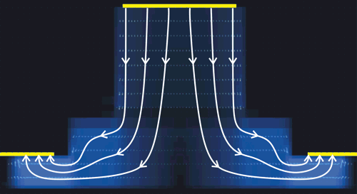
A material resistivity is assigned to each material used in the waveguide. PICWave can then automatically generate a resistive mesh to model current spreading in the simulation. The current flows down the central conductive channel, through the active layer, then laterally outwards to the ground contacts on each side. This is illustrated in the figure below.
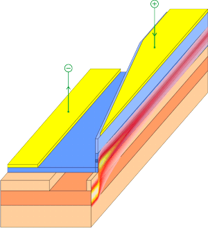
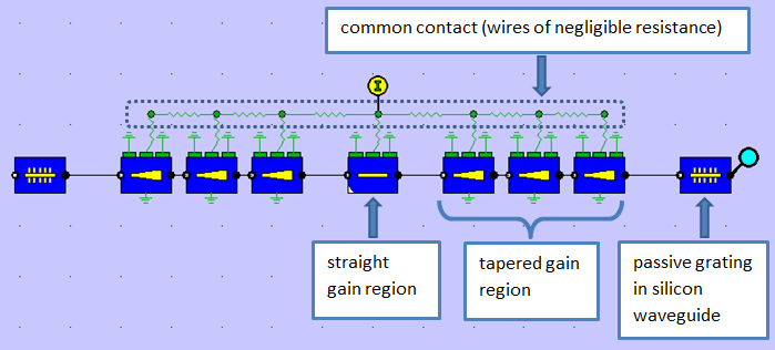
Tapered SOI laser diodeLight is commonly coupled out of such SOI hybrid lasers by linearly narrowing the III-V mesa region above the silicon waveguide. This adiabatically transforms the mode from the hybrid waveguide to the passive silicon waveguide.
This can be modelled in PICWave using active taper sections. The example below shows a hybrid DBR laser with a central straight gain region and tapered regions connecting to a DBR grating at each end, formed in passive silicon waveguides.
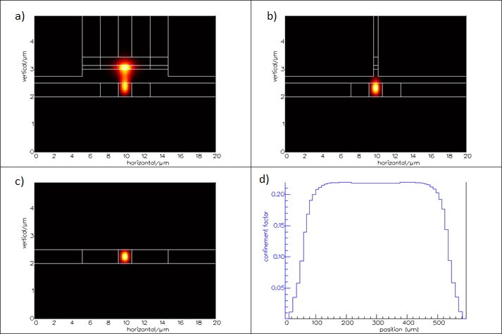
The optical mode at various points in the laser are shown below.
|

 © 2023 Photon Design copyright all rights reserved |

 |