|
|
Your source of photonics CAD tools | |
|
| ||
HaroldA hetero-structure laser diode model |
    |
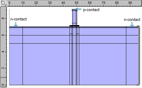
Hybrid Silicon Laser ModelSimulation with Harold XY softwareHarold’s XY Laser Module can be used to simulate Silicon-On-Insulator (SOI) hybrid lasers. In this example we simulate an hybrid silicon laser based on a design by UCSB. The structure has a III-V mesa region with an MQW AlGaInAs active region bonded to an SOI waveguide. The structure is ~70um wide in total with a 4um-wide central current channel, below which is an Si rib width surrounded by air channels on either side. The device was simulated in Isothermal mode (pulsed operation) from 0 to 500mA bias.
XY Cross-section XY Cross-sectionThe figure below shows the SOI hybrid structure that was set up in Harold.
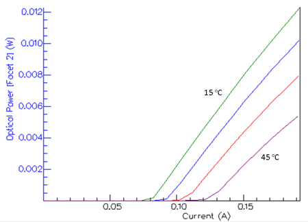
2D XY Simulation – basic characteristicsLike a Harold simulation, an XY simulation yields the basic characteristics of the device, such as the power-current relation for different temperatures. It is shown in the figure below for the simulated SOI hybrid laser structure.
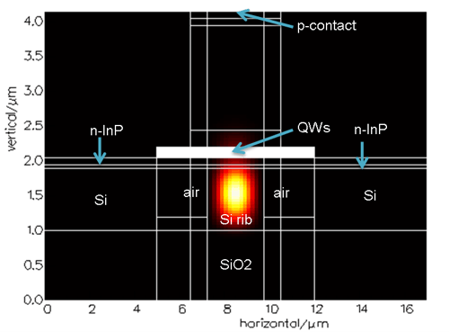
2D XY Simulation – optical modeThe XY Laser Module has a 2D FDM mode solver. The figure below shows the optical mode confined in this silicon rib waveguide; part of it overlaps with QWs, which provide optical gain for the lasing mode.
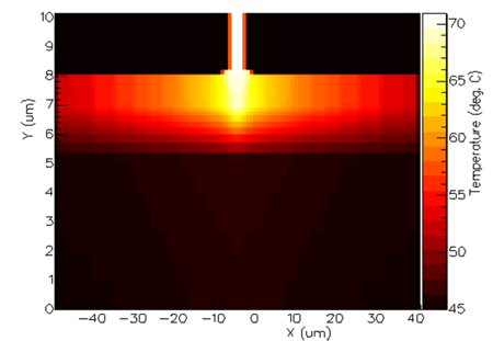
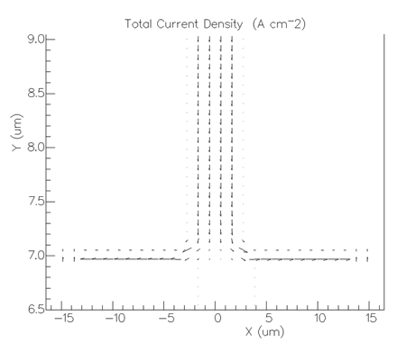
2D XY Simulation – profiles/current spreadingIn addition to basic device characteristics, an XY simulation yields numerous 2D profile results. A selection of those obtained from the SOI hybrid laser simulation are shown below.
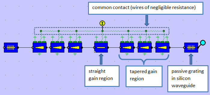
Modelling a tapered hybrid laser with PICWaveYou can model more complex geometries of hybrid lasers including tapered hybrid lasers (circuit shown below) using a combination of Harold and PICWave.
|
 © 2023 Photon Design copyright all rights reserved |

 |