|
|
Your source of photonics CAD tools | |
|
| ||
CrystalWaveA powerful photonic crystal simulator |
    |
Bloch Modes of a Photonic Crystal WaveguideSimulation with CrystalWave softwareCrystalWave can be used to design and simulate any kind of photonic crystal waveguide. In this case we are calculating the band diagram and identifying the Bloch modes of a photonic crystal waveguide, created by introducing a line defect in a square 2D photonic crystal lattice of vertical rods. The band diagrams, band gaps and Bloch modes were calculated using CrystalWave's Band Structure Analyser and the results validated using its FDTD Engine. Such simulations can performed in 2D and in 3D.
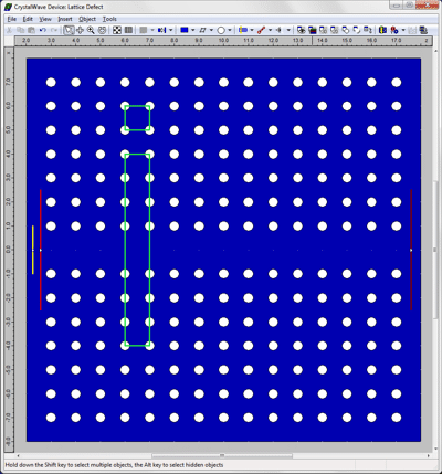
Design of the photonic crystal structureWith CrystalWave, designing and modifying a photonic crystal lattice is extremely easy. CrystalWave's editor comes packed with dedicated tools to create and modify 2D and 3D photonic crystal lattices, introduce point and line defects and offset lattice atoms from their ideal positions (offsets can be randomised for tolerance studies). Atom can be defined using a set of 2D and 3D shapes (ellipses, polygons, ellipsoids) which can be coated with a defined thickness. In order to design the 2D square photonic crystal below, we simply added a lattice to shape (one click) and changed the lattice angle and constants to fit our requirements. The lattice itself was filled with circular atoms and the line defect was created in two more clicks.
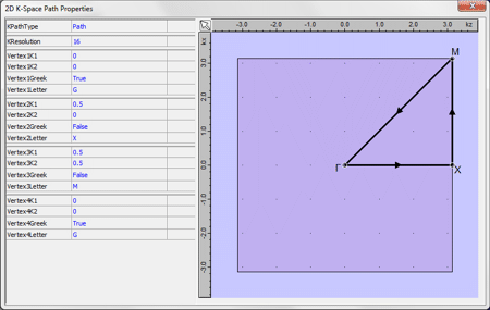
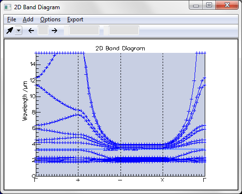
The lattice period was set to 1um and the hole diameter to 0.4um. The optical properties of the different regions were defined for 2D simulations. In this case the dark blue areas have a refractive index of 1 whilst the white rods have a refractive index of 3.4. Two different unit cells were added to the structure, in order to tell the Band Solver on which part of the device to perform the simulation. One of the unit cells selected a square unit of the lattice to identify the band gaps of the structure, whilst the other unit cell was placed across the defect to calculate the Bloch modes of the waveguide. An input waveguide, an excitor and some sensors were also added to perform an FDTD simulation on the same structure. Calculating the band diagram for the periodic structureThe band diagram for the periodic lattice was calculated with CrystalWave's Band Structure Analyser. The Brillouin zone was calculated and the irreducible Brillouin zone around which the calculation is performed was identified automatically; in this case the K-path is the conventional ΓXM path used for square lattices. It can be inspected and modified by the user from the panel shown below.
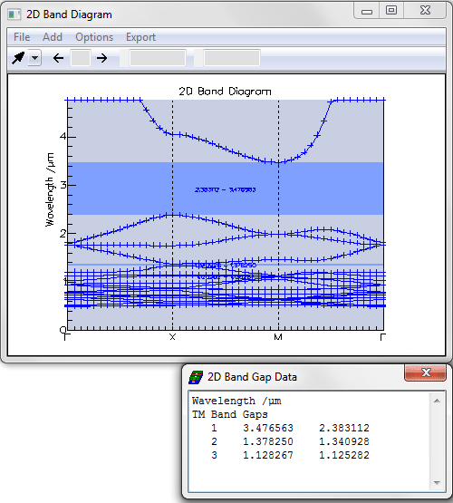
The band diagram was calculated for TM bands. The band diagram can be plotted against wavelength, absolute frequency or relative frequency; it is shown plotted against wavelength below. There is a large band gap for the TE polarisation between 2.383um and 3.476um.
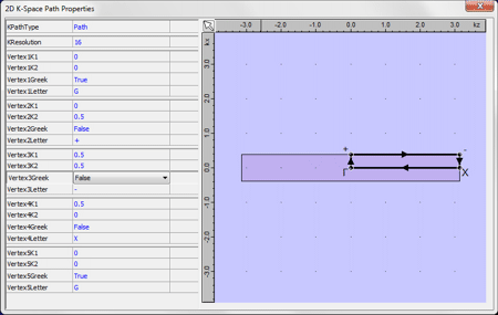
Calculating the guided Bloch modes using the Band Structure AnalyserWe then calculated the band diagram for the unit cell across the line defect lattice. Again, the Brillouin zone and the irreducible Brillouin zone were identified automatically. They can be inspected and modified by the user from the panel shown below.
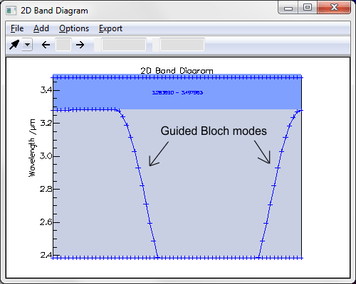
The band diagram was calculated for TM bands; it is shown plotted against wavelength below. The large band gap between 2.383um and 3.476um has disappeared and is now occupied by the bands corresponding to guided Bloch modes.
We can visualise the guided bands by displaying the part of the band diagram that overlaps with the band gap for the square lattice. This reveals the band along which the guided modes can be found. The first quarter of the data corresponds to kz=0, i.e. to the evanescent modes. In the second and fourth quarter of the band you can find the guided Bloch modes, which are supported for wavelengths varying between 2.3831um and 3.2839um, the lower limits of the band gap of the first and second unit cells, respectively. In the third quarter we find non-guided radiation modes.
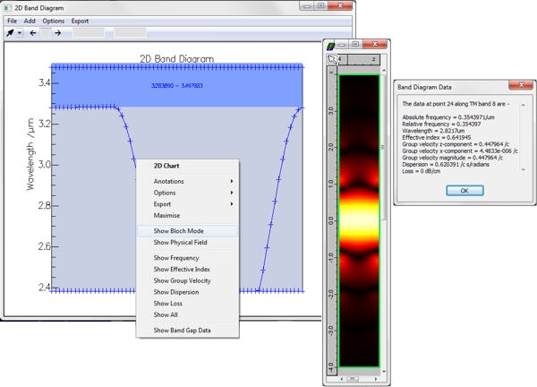
The field profiles and properties of the Bloch mode at a given band point can be inspected; a TM Bloch mode is shown below along with its properties (wavelength, effective index, group index, dispersion, mode loss etc.). The mode is very clearly confined within the lattice defect, which acts effectively as a waveguide for this range of wavelength.
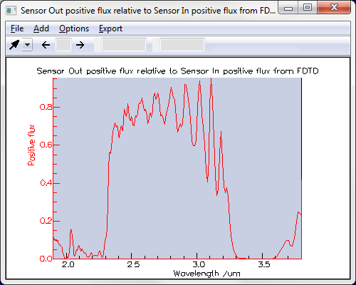
Exciting the guided Bloch modes using the FDTD EngineThe results were checked with an FDTD simulation. A sinusoidal pulse of light centred on the middle of the wavelength range that supports modes was launched from the excitor and a spectrum of the transmission through the photonic crystal region was generated. As expected, it shows that light is only transmitted for the wavelengths between 2.3831um and 3.2839um for which guided Bloch modes are supported.
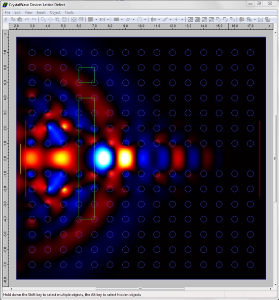
A screenshot showing the Ey field during the FDTD calculation is show below. The guided light can be seen very clearly.
|

 © 2023 Photon Design copyright all rights reserved |

 |